|
|
|
|
|
|
| Home | Company Info | Blog | Tutorials & Tools | Forums | Store | Services | Contact | Site Map |
Microstrip Patch Antenna |
From Simulation to RealizationIn the Ansoft HFSS Tutorial 1, a microstrip patch antenna was simulated and the numerical return loss and radiation patterns were shown. The purpose of this tutorial is to further discuss the microstrip patch antenna and to present the experimental results. In particular, the dimensions of the patch are given along with the feed network. Discussion of the dimensions and how they were obtained are presented. The fabricated microstrip patch antenna is also shown. The experimental return loss and the experimental E- and H-plane radiation patterns are compared with the Ansoft HFSS results. In addition, a three-dimensional radiation pattern of the fabricated antenna is also shown. The purpose of this tutorial is to show readers a comparison of numerical and experimental results. 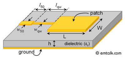
Figure 1. Model of microstrip patch antenna; edge-fed with quarter wavelength transformer section to 50 Ω transmission line. Microstrip Patch ModelThe microstrip patch antenna model used for the numerical simulation in Ansoft HFSS is shown in Fig. 1. The patch antenna is designed for 2.4 GHz operation on a substrate with 2.2 permittivity and 1.57 mm thickness. To determine the width (W), the microstrip patch antenna calculator was used to provide an initial starting point. The length (L) was chosen to be the same as W to obtain a symmetric radiation pattern. The patch without the feeding network was simulated in Ansoft HFSS to adjust W for resonance at 2.4 GHz. Next, the input impedance of the patch at the edge was determined by placing a length of 50 Ω transmission line at the edge. By de-embedding the 50 Ω transmission line, the edge input impedance was determined to be 343 Ω. Therefore, a quarter-wave length transformer was used to match 343 Ω input impedance to a 50 Ω system. The final dimensions of the entire microstrip patch antenna are
RealizationAfter the HFSS simulation confirmed a resonance of 2.37 GHz with a return loss less than -10 dB, the microstrip patch antenna was realized by photolithography. Fig. 2. shows the realized microstrip patch antenna with a 3.5 mm SMA female connector compared with the HFSS model. The comparison of the numerical and experimental return loss is shown in Fig. 3. Good agreement can be seen between HFSS and the measured results. 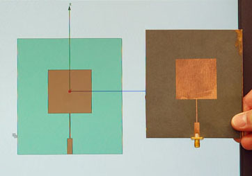
Figure 2. Micrstrip patch antenna: Model versus Reality. 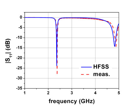
Figure 3. Return loss of the microstrip patch antenna. Radiation PatternThe fabricated antenna was then placed inside an antenna chamber. Fig. 4 shows the antenna mounted onto a rotational stage. A waveguide probe was used to measure the near-field of the microstrip patch antenna and post-processing was performed to obtain the far-field radiation patterns. 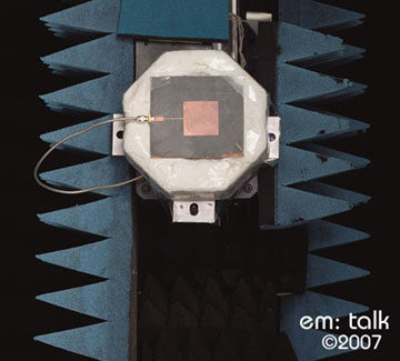
Figure 4. Fabricated microstrip patch antenna ready for near-field sampling. The numerical and experimental E- and H-Plane radiation patterns are shown in Fig. 5 and Fig. 6, respectively. Good agreement can be seen, discrepency on the backside is due to the metallic mounting structure of the antenna chamber's rotational stage. Fig. 7 shows the experimental 3-D radiation pattern of the microstrip patch antenna. 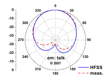
Figure 5. E-Plane radiation pattern. 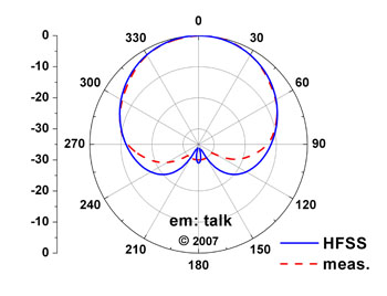
Figure 6. H-Plane radiation pattern. 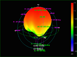
Figure 7. 3-D radiation pattern. Discuss this in the forums. |
|
em: talk © 2006-2010 | All Rights Reserved |
|