|
|
|
|
|
|
| Home | Company Info | Blog | Tutorials & Tools | Forums | Store | Services | Contact | Site Map |
HFSS Tutorial 1 |
Microstrip Patch AntennaHFSSv10 (download simulation file) The microstrip patch antenna is a popular printed resonant antenna for narrow-band microwave wireless links that require semi-hemispherical coverage. Due to its planar configuration and ease of integration with microstrip technology, the microstrip patch antenna has been heavily studied and is often used as elements for an array. In this tutorial, a 2.4 GHz microstrip patch antenna fed by a microstrip line on a 2.2 permittivity substrate is studied. The following topics are covered:
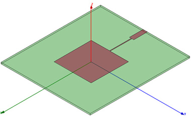
Model SetupFirst the model of the microstrip patch antenna has to be drawn in HFSS. It consists of rectangular substrate and the metal trace layer as shown in Fig. 1. Note that a quarter-wave length transformer was used to match the patch to a 50 Ohm feed line. The dimensions of antenna can be found in the HFSS simulation file.
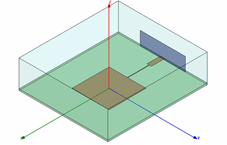
Waveport SetupIn order to excite the structure an excitation source has to be chosen. For this simulation a waveport will be used. The waveport will excite the first mode of the microstrip line (quasi-TEM) and then HFSS will use this field to excite the entire structure. In order to get an accurate result, the waveport has to be defined properly; if it is too small the field will be truncated (characteristic impedance will be incorrectly calculated) and if it is too large a waveguide mode may appear. Please refer to the tutorial on defining a waveport for further information. Since the substrate height is 1.57 mm and the feed line width is 4.84 mm, the waveport size chosen is 5 mm high by 50 mm wide. After the waveport rectangle is drawn, the WAVEPORT excitation was assigned to it. In the Analysis section of this tutorial, it will be shown that this waveport size accurately models the desired microstrip mode. Airbox and Boundary Conditions
An airbox has to be defined in to model open space so that the radiation from
the structure is absorbed and not reflected back. The airbox should be a
quarter-wavelength long of the frequency of interest in the direction of the
radiated field. In the directions where the radiation is minimal, this
quarter-wavelength condition does not have to be met and an air “space” may not
even have to be defined. Since the radiation of a patch antenna is concentrated
at broadside, a rectangular box enclosing the structure is only needed; the
height of the airbox is 31.25 mm (quarter-wave at 2.4 GHz). The antenna with
airbox and waveport setup is shown in Fig. 2.
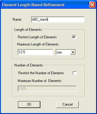
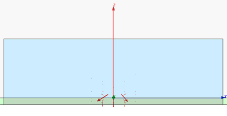
Next, the 4 side faces and the top face of the airbox were selected (Press F to select faces and O to select objects) and RADIATION boundary was applied. Then the bottom face and the patch antenna trace were selected and a FINITE CONDUCTIVITY boundary using Copper was assigned. MeshingManually meshing should be performed on the airbox to get accurate results for the antenna properties such as efficiency, directivity, and radiation pattern. One should seed the airbox lambda/10. For this structure the initial mesh length for the airbox was set to 12.5 mm (lambda/10 at 2.4 GHz). Fig. 3 shows the mesh property window.
Analysis/Sweep Setup
A Solution Setup is added to the analysis of the simulation with the
following:
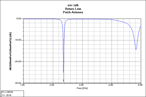
Plotting ResultsThe resulting return loss of the structure is shown in Fig. 5.
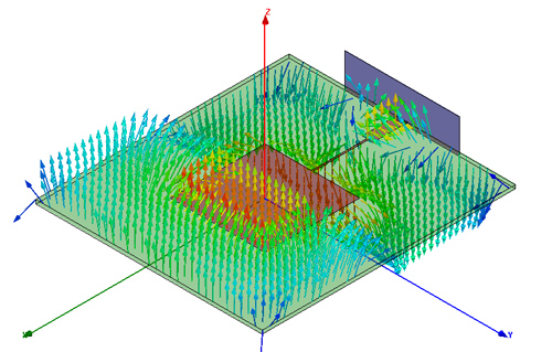
From Fig. 5, the fundamental resonance of the antenna occurs at 2.36 GHz with a return loss of -29.43 dB. Next, the top face of the substrate was selected and the Electric Field Vector was plotted for 2.36 GHz. The field plot is shown in Fig. 6 and shows the expected half-wavelength field distribution.
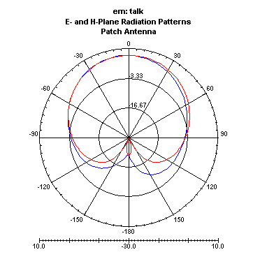
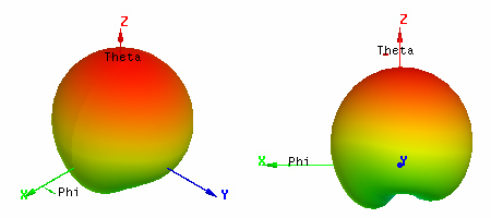
To plot the far-field patterns of the antenna, a far-field setup has to be created. Two will created; one for the E- and H-Plane two-dimensional patterns and another for the three-dimensional pattern. To create each far-field setup go to HFSS>Radiation>Insert Far-Field Setup>Infinite Sphere. For the two-dimensional pattern, the default values have to be changed; Phi should start at 0 deg and stop at 90 deg with a 90 deg step size. For the three-dimensional pattern, the default values can be used. Fig. 7 shows the two-dimensional patterns and Fig. 8 shows the three-dimensional patterns. To obtain the radiation efficiency, peak gain, etc. go to HFSS>Radiation>Compute Antenna/Max Param and choose 2.36 GHz as the frequency of interest.
Discuss this in the forums. |
|
em: talk © 2006-2009 | All Rights Reserved |
|